- 您现在的位置:买卖IC网 > Sheet目录3871 > PIC18F14K50-I/SO (Microchip Technology)IC PIC MCU FLASH 8KX16 20-SOIC
dsPIC30F1010/202X
DS70178C-page 242
Preliminary
2006 Microchip Technology Inc.
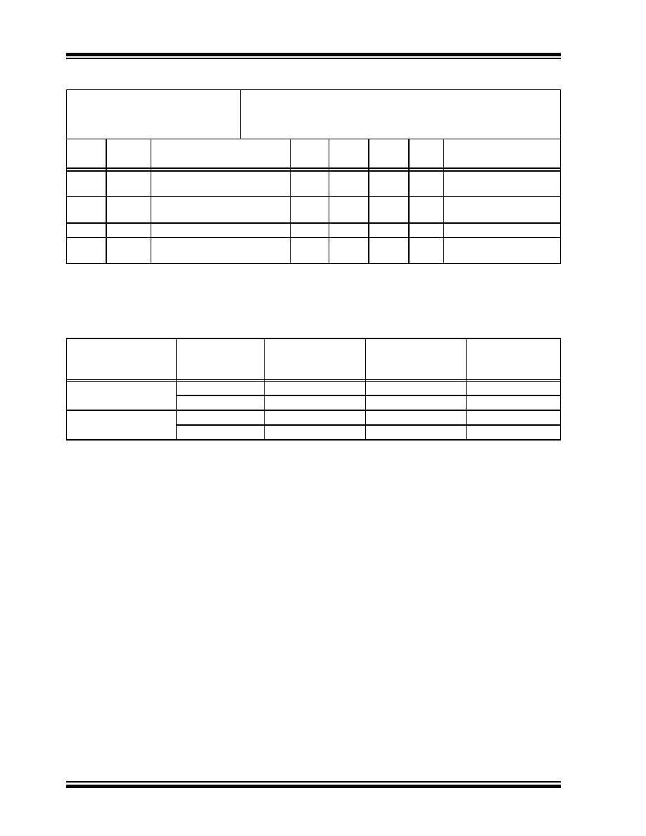
TABLE 21-13: PLL CLOCK TIMING SPECIFICATIONS (VDD = 3.0 AND 5.0V )
AC CHARACTERISTICS
Standard Operating Conditions: 3.3V and 5.0V (±10%)
(unless otherwise stated)
Operating temperature
-40°C
≤ TA ≤ +85°C for Industrial
-40°C
≤ TA ≤ +125°C for Extended
Param
No.
Symbol
Characteristic(1)
Min
Typ(2)
Max
Units
Conditions
OS50
FPLLI
PLL Input Frequency Range(2)
6
—
15
MHz
EC, HS modes with PLL
x32
OS51
FSYS
On-chip PLL Output(2)
192
—
480
MHz
EC, HS modes with PLL
x32
OS52
TLOC
PLL Start-up Time (Lock Time)
—
20
50
μs
OS53
DCLK
CLKO Stability (Jitter)
—
1
%
Measured over 100 ms
period
Note 1:
These parameters are characterized but not tested in manufacturing.
2:
Data in “Typ” column is at 5V, 25°C unless otherwise stated. Parameters are for design guidance only and
are not tested.
TABLE 21-14: INTERNAL CLOCK TIMING EXAMPLES
Clock
Oscillator
Mode
FIN (MHz)(1)
TCY (
μsec)(2)
MIPS(3)
w/o PLL
MIPS(4)
w/PLL x32
EC
10
0.2
5.0
20
15
0.133
7.5
30
HS
10
0.2
5.0
20
15
0.133
7.5
30
Note 1:
Assumption: Oscillator Postscaler is divide by 1.
2:
Instruction Execution Cycle Time: TCY = 1/MIPS.
3:
Instruction Execution Frequency without PLL: MIPS = FIN/2 (since there are 2 Q clocks per instruction
cycle).
4:
Instruction Execution Frequency with PLL: MIPS = (FIN * 2).
发布紧急采购,3分钟左右您将得到回复。
相关PDF资料
PIC16F628A-I/SS
IC MCU FLASH 2KX14 EEPROM 20SSOP
PIC18LF43K22-I/PT
IC PIC MCU 8KB FLASH 44TQFP
DSPIC33FJ16MC101-I/SO
IC DSP 16BIT 16KB 20SOIC
PIC12C672-04I/SM
IC MCU OTP 2KX14 A/D 8-SOIJ
PIC12C671-04I/SM
IC MCU OTP 1KX14 A/D 8-SOIJ
PIC18F26K20-I/SO
IC PIC MCU FLASH 32KX16 28-SOIC
PIC18LF24J11-I/SO
IC PIC MCU FLASH 16K 2V 28-SOIC
DSPIC33FJ16MC102-I/SS
IC DSP 16BIT 16KB 28SSOP
相关代理商/技术参数
PIC18F14K50-I/SS
功能描述:8位微控制器 -MCU 16KB Flash 768 RAM15 I/O 10-B ADC USB 2.0
RoHS:否 制造商:Silicon Labs 核心:8051 处理器系列:C8051F39x 数据总线宽度:8 bit 最大时钟频率:50 MHz 程序存储器大小:16 KB 数据 RAM 大小:1 KB 片上 ADC:Yes 工作电源电压:1.8 V to 3.6 V 工作温度范围:- 40 C to + 105 C 封装 / 箱体:QFN-20 安装风格:SMD/SMT
PIC18F14K50T-I/SO
功能描述:8位微控制器 -MCU 16KB Flash 768 RAM15 I/O 10-B ADC USB 2.0
RoHS:否 制造商:Silicon Labs 核心:8051 处理器系列:C8051F39x 数据总线宽度:8 bit 最大时钟频率:50 MHz 程序存储器大小:16 KB 数据 RAM 大小:1 KB 片上 ADC:Yes 工作电源电压:1.8 V to 3.6 V 工作温度范围:- 40 C to + 105 C 封装 / 箱体:QFN-20 安装风格:SMD/SMT
PIC18F14K50T-I/SS
功能描述:8位微控制器 -MCU 16KB Flash 768 RAM15 I/O 10-B ADC USB 2.0
RoHS:否 制造商:Silicon Labs 核心:8051 处理器系列:C8051F39x 数据总线宽度:8 bit 最大时钟频率:50 MHz 程序存储器大小:16 KB 数据 RAM 大小:1 KB 片上 ADC:Yes 工作电源电压:1.8 V to 3.6 V 工作温度范围:- 40 C to + 105 C 封装 / 箱体:QFN-20 安装风格:SMD/SMT
PIC18F2220-E/SO
功能描述:8位微控制器 -MCU 4KB 512 RAM 25 I/O RoHS:否 制造商:Silicon Labs 核心:8051 处理器系列:C8051F39x 数据总线宽度:8 bit 最大时钟频率:50 MHz 程序存储器大小:16 KB 数据 RAM 大小:1 KB 片上 ADC:Yes 工作电源电压:1.8 V to 3.6 V 工作温度范围:- 40 C to + 105 C 封装 / 箱体:QFN-20 安装风格:SMD/SMT
PIC18F2220-E/SP
功能描述:8位微控制器 -MCU 4KB 512 RAM 25 I/O RoHS:否 制造商:Silicon Labs 核心:8051 处理器系列:C8051F39x 数据总线宽度:8 bit 最大时钟频率:50 MHz 程序存储器大小:16 KB 数据 RAM 大小:1 KB 片上 ADC:Yes 工作电源电压:1.8 V to 3.6 V 工作温度范围:- 40 C to + 105 C 封装 / 箱体:QFN-20 安装风格:SMD/SMT
PIC18F2220-I/SO
功能描述:8位微控制器 -MCU 4KB 512 RAM 25 I/O RoHS:否 制造商:Silicon Labs 核心:8051 处理器系列:C8051F39x 数据总线宽度:8 bit 最大时钟频率:50 MHz 程序存储器大小:16 KB 数据 RAM 大小:1 KB 片上 ADC:Yes 工作电源电压:1.8 V to 3.6 V 工作温度范围:- 40 C to + 105 C 封装 / 箱体:QFN-20 安装风格:SMD/SMT
PIC18F2220-I/SO
制造商:Microchip Technology Inc 功能描述:IC 8BIT FLASH MCU 18F2220 SOIC28
PIC18F2220-I/SOC03
制造商:Microchip Technology Inc 功能描述: